Sigma EF-500 DG SUPER MA(Minolta) Modification for the Pentax Hot Shoe Mount

이번 삽질도 아트와 관련된 거다.
내가 원래 아트에 관심이 좀...

재활용 쓰레기통에서 망가진 외장 플래시를 구했다.
모델명은 'Sigma EF-500 DG SUPER MA'로 보인다.
확인해 보니 플래시 램프가 타버렸다.
가지고 있는건 펜탁스 카메라인데, 이건 Minolta 마운트용이다.
[Fig. 1] 처럼 생겼다.

I've finished the conversion of the 'Sigma EF-500 DG SUPER MA' Minolta hot shoe mount into the Pentax hot shoe mount. And I'll describe what I've done about it.
My Sigma EF-500 DG SUPER MA's flash lamp was burned out so doing the lamp replacement is initial process and then, I have to modify mechanical-mounting followed by electrical-mounting.
I did not took pictures during the flash lamp replacement.
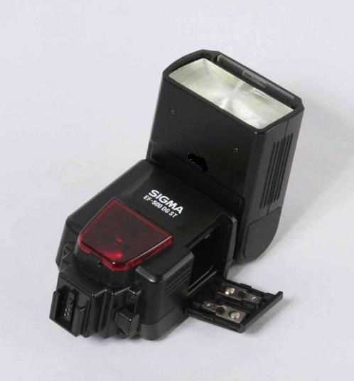

[Fig. 1 Sigma EF-500 DG Minolta Mount]

펜탁스에 붙여서 사용하려니 3가지 작업을 해야한다.

1. 타버린 램프를 교체
2. 기계적 마운트롤 교체
3. 전기적 마운트도 교체

음.. 일이 많다.
가지고 있던 싸구려 외장 플래시에서 램프를 빼내어 교체작업을 한다.
플래시 분해는 아래 사이트를 참고 했다.

You can refer to below link to disassemble the strobe.

Repairing an erratic Sigma EF500 DG ST
(Thank you weijen)


[Fig. 2 Extracted Burned Flash Lamp]


[Fig. 3 Hot Shoe Mount Replacement]

교체후 타버린 플래시 램프 사진만 찍었다
램프 교체하고 테스트를 해보니 동작은 잘 된다.
기계적 마운트역시 가지고 있던 외장 플래시에서 마운트 부분을 떼어내 붙여 준다.
자, 이제 전기적 마운팅을 해줘야 하는데 자료를 뒤져 보니 이거 만만치가 않다.
그냥 strobe signal을 접지 시키면 될 줄 알았는데 그렇지가 않다.
특히나 Minolta 방식이 까다로운가 보다.
전기적 마운팅을 위해 아래 3개 사이트를 참고 했다.

I've checked it works well after repairing the flash lamp, and have modified the mechanical mount with parts from my cheap external strobe for the Pentax.
Next step is just electrical-mounting but I've been aware of danger of this job. There are no easy way to trigger this strobe manually just like shorting the fire signal to the ground.
I've found out very useful 3 links bellow for this.

adrian        : Hacking the Sigma EF-500 DG Super strobe Part 1/2
Kimmo Kulovesi: Sigma EF-500 DG Super PC-sync port modification
Impulsite     : Sigma EF-500 DG ST, есть схема
(Thank you adrian, Kimmo Kulovesi and Impulsite)

adrian 링크는 수동으로 플래시를 동작 시키기 위해 겪은 시행착오를 공유해 놓은 내용이고 Kimmo Kulovesi 링크는 adrian의 시행 착오에 15nF 커패시터를 추가하여 개선했다는 내용이다. Impulsite 링크는 플래시 회로도를 공유해 주었다.
3명의 자료 공유 덕분에 내 작업이 비교적 순조롭게 진행 될 수 있었다.
얼굴도 모르는 세계의 3분에게 다시한번 감사드린다. 소중한 시간을 아낄 수 있었다.

I think the adrian is a pioneer of the Sigma EF-500 DG modification. He suggested really good idea for manual trigger through the optical-slave mode of the strobe and this method works well. All images are broken when I visit the adrian's site, but you can search images by image-googling with 'Hacking the Sigma EF-500 DG Super strobe' key words.
Kimmo Kulovesi improved the unstable behavior by attaching 15nF capacitor for bypassing noise, also very nice recommendation.
Impulsite's web is very useful with strobe's schematics.
I could make a conversion into the Pentax mount successfully by these informaion only in 2 days. I hope to say thank you adrian, Kimmo Kulovesi and Impulsite again, you saved my time.
Additionally, I performed several invetigation and experiments to make it clear. When I shorted the photo-diode's anode and cathod, large current was observed by probing the voltage drop with my strobe, so I added current limiting register in my final result, R1 in [Fig. 7].
General Si. photo-diodes let current under 100uA, typically 50~60uA, when detected the light.
The main CPU should observe the delta-voltage, approximatly under a hundred micro-volts to detect the light if there is no signal amplification.
I found that the photo-diode's singal (anode) is routed to the main CPU(?) directly, it's means that the main CPU(?) may detect under 100uV of delta-volts to sync with light signal when it's in optical-slave mode.
The strobe's unstable behavior (without Kimmo Kulovesi's 15nF capacitor) could be explained by this measurement mechanism. If you extended the photo-diodes's signal wire (anode), even small disturbances could influence the delta-micro-volts detection loop so the Kimmo Kulovesi's 15nF capacitor is very important.
To protect DSLR camera I attached the opto-coupler PC817.
You should short pin 5 and 6 to work properly in optical-slave mode. refer to [Fig. 8].
My Pentax camera and the modified Sigma EF-500 DG SUPER MA works perfectly togather in "C0 SL" mode.

요약하자면 다음과 같다.

1. Sigma EF-500 DG SUPER는 단순 단락으로 플래시 동작이 안된다.
2. optical-slave모드에서 내부 photo-diode 신호를 변형해 동작이 가능하다.
3. photo-diode 신호 변형을 위해 wire를 인출 하면 동작이 이상해 진다.
4. 인출된 wire에 커패시터를 부착하면 사용가능한 수준이 된다.

adrian이 말한대로 photo-diode에서 선을 빼내면 수동으로 동작이 가능하지만, 가끔 플래시가 먹통이 된다. 이를 위해 Kimmo Kulovesi는 신호선에 15nF 커패시터를 달아 해결하였다.
Impulsite의 회로도를 참고해 나름 테스트를 해본 결과 photo-diode의 신호를 메인 CPU(?)에서 입력 받는 구조인데, photo-piode의 전류 신호가 수십 uA대로 작다 보니 측정되는 전압의 변화 역시 수십uV 수준이다.
외부에 선을 달아 주게 되면 안테나 역할을 하게 되면서 외부 노이즈가 유입되어 플래시 커패시터의 방전과 충전이 반복되면서 기기가 먹통이 된다.
처음에 adrian이 소개한 대로 photo-diode의 선을 인출 하여 쇼트시켜보니 동작은 하는데 전류가 많이 흐르는듯 하다. 하여, 아래와 같이 카메라도 보호할 겸해서 opto-coupler를 추가로 장착하여 카메라와 연동하는데 성공 했다. [Fig. 7]에서 추가한 R1은 과전류 보호용이고 R2는 opto-coupler의 발광 다이오드 구동용이다.
optical-slave 모드로 동작 시키기 위해서는 [Fig. 8]과 같이 커넥터 5번과 6번을 쇼트 시켜야 한다.
플래시의 발광량 가변이 되니 신세계다.


[Fig. 4 Power board, Pic. from Impulsite]


[Fig. 5 Power board Schematics, Pic. from Impulsite]


[Fig. 6 Photo-Diode Polarity, Anode(A) and Cathod(C)]


[Fig. 7 Modification Schematics]


[Fig. 8 Connector Modification]

Hot shoe connector pin out
  - 1  : F2 (READY)
  - 2  : F1 (SYNC/FIRE)
  - 3  : GND
  - 4  : F3 (TTL OK)
  - 5/6: Shoe Mount Detection (contacted together when demounted)
  - 7/8: LED

[Fig. 9 Wiring]


[Fig. 10 Final Result]

사진은 안찍고 이런거나 만들고 있음.

DIY Footswitch for the Line6 POD

역시 간만에 또 글을 쓰는군.
이번 삽질은 아트와 관련된 거다.
전기기타 멀티이펙터용 풋스위치.

얼마전 Line6사의 POD 전기기타용 멀티이펙터(정확한 명칭은 앰프 시뮬레이터라고함)를 구했다.
꾹꾹이만 쓰다 멀티이펙터를 사용해 보니 우와 편하고 좋다.
근데 풋스위치가 없어서 좀 불편하다.
검색해 보니 누군가 POD의 풋스위치 인터페이스에 대해 나름 숭고한 삽질의 결과를 친히 공개해준 자료가 있어 많은 도움이 되었다.

In this text, I hope to share my private project result 'DIY Footswitch for the Line6 POD' which was motivated by Mark Lavelle's great effort and time sharing.

http://harmonicappliances.com/floorboard/floorboard.html
(시간과 노력을 공유해준데 대해 대단히 감사드립니다.)
(Very very thank you Mark Lavelle for your great job and publication.)

초기 계획은 LED빼고 저항과 스위치만으로 구성하여 간단하게 맹글어 쓸려고 했는데 기왕이면 LED 불도 켜지면 좋을꺼 같고, 7-segment로 숫자도 표시되면 좋을꺼 같고해서 마침 놀고 있던 PIC18F2550을 활용해 만들었다.

풋스위치는 아래와 같이 외부에 저항만 직렬 연결하면 구성이 된다.

As described above link, footswitch functions are enough just with passive series-resistors.
===========================================================
      POD
  ----------+
            |
       5V   |
       |    |
       R=1K |
       |    |  RJ-45 pin 6
  AD(?)+-------+
            |  R1=0
  ----------+  +------SW-----GND : TapTempo/Tuner(0.04V)
               R2=100
               +------SW-----GND : ChSel/EffectOnOff(0.49V)
               R3=120(220)
               +------SW-----GND : Wah(0.90V)
               R4=150(370)
               +------SW-----GND : ChA/EQ(1.38V)
               R5=200(570)
               +------SW-----GND : ChB/TremChorus(1.83V)
               R6=240(810)
               +------SW-----GND : ChC/Delay(2.23V)
               R7=290(1.1K)
               +------SW-----GND : ChD/Reverb(2.67V)
               R8=1.6K(2.7K)
               +------SW-----GND : BankUpDown(3.65V)
               R9=1.0K(3.7K)
               +------SW-----GND : BankUp(3.88V)
               R9=1.3K(5.0K)
               +------SW-----GND : BankDown(4.1V)
               R10=15K(20.0K)
               |
              GND
===========================================================

채널 4개 선택, Bank-Up, Tuner스위치만 구성했다.
LED구동을 하려면 위 링크에 설면된 대로 POD에서 보내주는 펄스 신호의 길이를 측정해야 한다. 때문에 별도 신호처리를 위한 장치가 있어야 하는데 PIC18F2550을 활용해 SW로 처리했다.
외부 4MHz오실레이터 입력을 받아 내부 PLL에서 48MHz(최대)로 동작 한다.
POD의 신호를 외부 인터럽트나 캡쳐 기능을 활용해 시간 측정을 하려고 시도했었으나, PIC의 인터럽트 지연(interrupt latency)이 의외로 길어 1us의 펄스신호를 측정하는데 부적합 했다(라고 썼지만 코드 최적화 능력이 안된다고 해석하면 된다). 그래서 메인루프에서 폴링기반으로 신호를 측정 하도록 구성했다. 이렇게 구성하니 interrupt context switching overhead가 없으므로 1us의 펄스 측정이 가능하였다.

I integrated channel A/B/C/D and only Bank-Up, Tuner switches for simplicity.
LED driving is not simple work, this function is needed a special device to handle digital pulses. I used PIC18F2550 micro-controller-unit to process digital pulses from the POD.
My initial design was concerned about display 3-digit 7-segment that is essential the timer interrupt based dynamic drive. But the 48MHz(maximum) clocked PIC18F2550 and my C-code could not measure the 1us pulse through the external interrupt/capture because of interrupt latency(Or maybe caused by my poor code optimization skill or non-asm code-base). So I've changed interrupt based code to polling method to measure 1us POD's LED pulses.
There is no interrupt context switching overhead in the polling method and for keeping up the regular sampling time, the code should not include any interrupt.

PIC18F2550 핀맵은 아래와 같다.
PIC18F2550 pin usage is like below.
========================================
  01[VPP] :VPP         28[RB7]:PGD
  02[RA0] :SEG_A       27[RB6]:PGC
  03[RA1] :SEG_B       26[RB5]:PGM
  04[RA2] :SEG_C       25[RB4]:LED_D
  05[RA3] :SEG_D       24[RB3]:LED_C
  06[RA4] :SEG_E       23[RB2]:LED_B
  07[RA5] :SEG_F       22[RB1]:POD_IN
  08[VSS] :GND         21[RB0]:LED_A
  09[OSC1]:4MHz        20[VDD]:5VDC
  10[OSC2]:4MHz        19[VSS]:GND
  11[RC0] :SEG_G       18[RC7]:UART-RX
  12[RC1] :LED_TEMPO   17[RC6]:UART-TX
  13[RC2] :NC          16[RC5]:NC
  14[VUSB]:NC          15[RC4]:NC
========================================

PIC구성시 초기 계획은 3-digit 7-segment를 활용하려 했으나, 폴링모드로 구성하는 바람에 7-segment의 dynamic drive구현이 불가능 하여 1-digit 7-segment만 적용했다. 때문에 POD에서 날라오는 신호값을 확인하여 각 모드에서 3개 문자중 필요한 것만 표기되도록 하였다.
POD의 튜너모드에서는 'Line6 Floor Board'처럼 6개 LED가 피치값을 표기해 주도록 되어있다. 그러나 내가 만든 footswitch에는 4개 LED밖에 없어 6개 LED 피치 디스플레이를 4개 LED로 압축하여 표기되도록 구성 했다.
7-segment를 비롯해 모든 LED는 active-low로 동작 한다(0일때 켜짐).

All LEDs including 7-segment are active-low(turned on when 0V, driven by sink current).
The LED_TEMPO was connected to dot-LED of the 7-segment.
Since my footswitch has only 4 LEDs and 1-digit 7-segment display, my code check the POD's current working mode to display only 1-digit, especially in tuner mode 6-LED based pitch display is shifted 4-LED based pitch display like below.

Line6 Floor Board의 튜너모드에서 LED 표기
LED display formula at the 'Line6 Floor Board' in tuner mode
===============================
  DIST_LED: lowest-pitch
  DRV_LED : lower-pitch
  CHA_LED : tuned/low-pitch
  CHB_LED : tuned/high-pitch
  CHC_LED : higher-pitch
  CHD_LED : highest-pitch
===============================

자작한 풋스위치의 튜너모드에서 LED 표기
My footswitch's LED display formula in tuner mode
===============================
  CHA_LED : lower-pitch
  CHB_LED : tuned/low-pitch
  CHC_LED : tuned/high-pitch
  CHD_LED : higher-pitch
===============================


[최종완성, Final Result]


[POD 연결부, POD Connection Side]


[Manual Mode]


[Channel-B at the Bank-9 in Preset Mode]


[Tuner Mode]


[5번줄(라) 튜닝, Tuned State with 5th(A) String]

튜너 모드에서 flat되었을때 POD에서는 flat표기를 해주지만 내 footswitch에서는 인지가 되지 않고 있다. TapTempo/Tuner LED를 flat표기로 변경해 주어야 겠다.

기타 연습은 안하고 이런거나 만들고 있음.


자작한 코드와 빌드된 헥사 파일을 첨부합니다.
115200bps 8N1으로 UART(RC7/RC6) 연결하면 문자로 동작 상태 모니터링 가능합니다.
리눅스에서 sdcc-3.6.0과 gputils-1.5.0-1로 빌드되었습니다.
개인적으로 자유롭게 사용하세요, 다만 상업적 이용은 금지합니다.

Present version of my footswitch does not display flat-pitch in tuner mode. Fortunately the POD send the flat-pitch tuned information by character 'b' by the right 7-segment LED pulse data. I'll update my code to display 'flat' through the dot-LED in 7-segment instead Tuner indication when tuner mode in someday...
I attached my code and hex file pre-built by sdcc-3.6.0 and gputils-1.5.0-1 at linux.
You may monitor the loop messages from PIC when connected with UART(RC7/RC6) at 115200bps 8N1.
You can use/modify my code/hex file freely but DO NOT use for commercial purpose.

code file: download
hex file : download

President Moon


요새 뭐 좀 비싼 카메라 메고 댕김서 펜대들고 설치는 놈들,
혓바닥이 걸레 쪼가리인건지 주둥아리로 쓰레기를 토해 내던데,

내가 뽑은 대통령이다.
건들지 마라.

무조건 지지

TCC8935 based Android IPTV hack/reverse-engineering

오~~ 요번글 제목도 괜찮다.
재활용 쓰레기장서 아래 그림처럼 희한하게 생긴걸 하나 주웠는데 인터넷TV 셋톱박스라는 구만.
근데 외부에 버튼 하나 없다.
아마 적외선 리모컨으로 조작하는가 본데 리모컨이 없으니 켜보지도 못하겠다.
모델명으로 검색해 봐도 안드로이드 기반의 IPTV라는거 말고는 당최 쓸만한 자료가 나오질 않는다.
제작사 홈페이지도, 공식 펌웨어도 못찾겠다.


[FIG.1 KM1100 Amway(Daum) IPTV mini]

[FIG.2 Main board]

[FIG.3 Component-side]

[FIG.4 Bottom-side]


  뭐 들어있나 배를 따봤다. 내부가 썰렁하다.
  CPU하나, 1GB DDR메모리, WIFI + Bluetooth 칩하나, 그리고 4G짜리 마이크로 SD카드 하나 달려있다. NAND나 NOR가 없는것으로 보아 SD로 부팅하는거 같다.
  CPU 모델명이 TCC8935라고 써있는데 검색해 보니 1GHz짜리 ARM Cortex A9프로세서다. 거기에 듀얼코어다. 우와... 메모리도 1GB에 안드로이드를 올릴 수 있다. 우와...
  안드로이드 함 올려볼까 하고 자료를 뒤적거려 봤다. 해당 칩으로 개발이 가능한 소프트웨어 패키지가 유출된적이 있었는데 지금은 구할 수가 없다.

  I've got an Android based IPTV H/W from recycle trash can that has a TCC8935 marked 1GHz ARM Cortex A9 processor, an 1GB DDR memory, an WIFI + Bluetooth chip and a 4GB micro-SD card, refer to [FIG.1], [FIG.2], [FIG.3] and [FIG.4]. It seems to be booted with micro-SD since there is neither NOR nor NAND.
  I could not turn the power it on because of absence of IR remote controller, so couldn't check it's ok or not (There is no hardware power botton).
  I found a web page that commenting about the TCC8935 and leaked development SW package but the leaked file has been gone.


  해당 웹페이지 글 내용으로만 봐서는 저것만 있으면 모든게 술술 풀릴듯 한데 아쉽게도 현재는 구할 수가 없다. 어쩔수 없이 삽질을 시작 했다.
  기본적으로 SD부팅을 하는데 SD카드를 제거하면 USB 부트모드로 진입가능하고 OS에서 신규 디바이스로 인식한다. USB 부트모드를 활용하면 될듯 하여 자료를 뒤져 봤으나, USB 부팅에 대한 자세한 내용은 역시 찾을 수가 없다.
  VTC라고하는 드라이버와 FWDN이라고 하는 SW를 가지고 펌웨어 업데이트등 조작이 되는듯 한데, 역시나 FWDN SW에 대한 USB프로토콜등 자세한 관련내용이나 자료도 없다.
  CPU벤더가 중국회사인줄 알았는데 Telechips라고 하는 한국에 있는 회사였다. 회사 홈페이지에 가봐도 의무적으로 공개해야하는 포팅된 리눅스 커널이외 쓸만한 자료는 없었다.
  개발자의 접근을 용이하게 해주면 더 잘 팔릴텐데...
  여튼, 도움이 될만한 자료가 거의 전무하다.
  보드에 TP가 몇개 보이길레 몇 군데 찔러보고 UART 핀을 찾아내고, 힌트가 될 만한 VTC/FWDN을 붙잡고 시작해봤다.
  구해진 VTC드라이버는 구버전이라 TCC8935를 지원하지 않는다. VTC드라이버 패키지에서 '*.ini' 파일을 찾아 TCC8935의 USB VIP/PID(0x140E/0xB098)를 쑤셔넣고 강제로 드라이버를 인식 시켰다.
  FWDN SW를 구동하면서 USBpcap(http://desowin.org/usbpcap)으로 USB패킷을 모조리 수집한 후 USB bulk-in/out 패킷을 분석하였다. 패킷 분석을 통해 내용을 대충 알아내고, libusb를 사용해 CPU에 코드를 쑤셔넣어 가면서 테스트 후 자작한 부트로더를 올릴 수 있었다.
  먼저 USB 패킷 크기는 512바이트이고, 2종류로 구성된다. 하나는 헤더 패킷, 두번째는 칩에 다운로드할 펌웨어 바이너리 패킷으로 구성된다. 헤더 패킷 포멧은 아래와 같다.

  There are some TPs at the board, and after digging, I found UART pin from the board. When I plugged the micro USB cable for power on, I could receive the bootloader and linux/Android kernel boot messages. Yes, the board is OK, but it's booted again and again. Probably the file system has been crashed.
  It's hard to find useful information about the development or firmwares on the net. I've googled for a few days but no luck without outdated VTC driver and FWDN for Windows.
  That VTC driver I've got was not support the TCC8935. Moreover there is no detailed user manual for the FWDN. After modification of the '*.ini' file, I could install the device driver with outdated-VTC driver compulsorily in Windows.
  I decided to analyze the USB packet with USBpcap(http://desowin.org/usbpcap).
  After digging with the USB packets for the FWDN and compulsory installed VTC driver through USBpcap and test code injection, I've found out working USB protocol format. First of all, USB bulk-in/out size is 512byte.
  The USB transaction is seperated into two parts, one is header and the other is main body for binary data transfer. USB header packet is like below.


  +--------------------------+
  | 32bit header key-code    | -> 0xf0000000, 0xf0000001
  +--------------------------+
  | 32bit download size      | -> download binary size in byte
  +--------------------------+
  | 32bit start address      | -> jump address after download
  +--------------------------+
  | 32bit download address   | -> download address
  +--------------------------+


  헤더 전송 이후 바이너리 데이터를 USB로 전송하면 된다. 코드로 구현하면 아래와 같다.

  After sending the USB header, you can send the binary code. This sequence is same as older TCC7xx or TCC8xx series but the header is little different.


  ---------------------------------------------------------
  unsigned int head[512>>2]= { 0, };
  ...
  p_dev= dev_open();  // device open
  ...
  // send header
  head[0]= key_code;
  head[1]= bin_size;
  head[2]= start_addr;
  head[3]= load_addr;
  usb_bulk_write( p_dev, 0x01, (char*)&head[0], 512, 500 );
  usb_bulk_read( p_dev, 0x82, (char*)p_rx, 512, 500 );
  ...
  ...
  // send binary
  usb_bulk_write( p_dev, 0x01, (char*)p_bin, bin_size, 5000 );
  usb_bulk_read( p_dev, 0x82, (char*)p_rx, 512, 500 );
  ...
  ---------------------------------------------------------
  key_code  : 0xf0000000 or 0xf0000001
  bin_size  : binary size in byte
  start_addr: jump address after download
  load_addr : download address
  p_dev     : USB device handle
  512       : USB bulk-in/out size
  500       : timeout in ms


  USB bulk-out이후 반드시 bulk-in을 읽어줘야 정상적으로 동작 되었다.
  헤더의 key-code가 FWDN 패킷 분석시 0xf0000000, 0xf0000001, 0xf0000006이 식별되었다. key-code가 0xf0000000일 경우 start address로 명시된 주소지를 콜한다. 무조건 분기가 아니고 함수 호출 형태이다. key-code가 0xf0000001일 경우 start address를 콜하지 않는다. 그냥 메모리로 다운로드만 한다. 패킷 분석시 0xf0000006도 있었는데 이건 뭔지 모르겠다 (메모리 읽기?). 여기서 중요한게 0xf0000000와 0xf0000001를 잘 사용하는 것이다.
  CPU 부팅시 DDR 메모리는 초기화가 되어 있지 않으므로 DDR메모리로 커널이나 부트로더등을 다운로드 할 수가 없다. 이때 0xf0000000을 이용해 내부 램에 DDR을 초기화 하는 코드만 전송하고, 두번째는 0xf0000001을 이용해 리눅스 커널을, 세번째는 다시 0xf0000000을 적용하고 부트로더를 전송후 부트로더로 점프하면 된다.
  USB 부트모드에서 CPU로 다운로드하기 위한 프로그램(usb_loader.exe)을 만들었다. 이 글 마지막에 드라이버와 프로그램 다운로드 링크를 걸어 둔다.
  자작한 usb_loader.exe 프로그램은 '-h', '-l', '-s', '-f'의 옵션 사용이 가능하다.

  There are several header key-code, 0xf0000000, 0xf0000001, 0xf0000006. Key-code 0xf0000000 is for download firmware and call the address that has been specified by start address in the header. I figured out that the CPU calls like a C-function call, it's not an unconditional JUMP with 0xf0000000 header key-code. Key-code 0xf0000001 is for just download, nothing happened after download with 0xf0000001 header key-code. There was 0xf0000006 key-code at the captured USB packet but I couldn't figured out what is this for. (memory read?)
  Calling usb_bulk_read() was mandatory after usb_bulk_write() in my test and always 4byte is returned with usb_bulk_read().
  I've made my own USB downloader(usb_loader.exe) for the TCC8935 from my USB packet digging result. It's uses libusb.
  You can download my USB downloader at the end of this text.
  The '-h', '-l', '-s', '-f' options are available for this program.


  -h: 0xf0000000 or 0xf0000001
  -l: download address
  -s: jump address after download
  -f: binary file


  자작한 프로그램으로 아래와 같이 사용 할 경우 리눅스와 부트로더가 DDR에 적재되고 부트로더로 점프할 수 있다.

  You can boot the TCC8935 CPU with bootloader/linux like below sequence. 4byte returned data is always 0x00000000 with 1st and 2nd download, but 0xffffffff after 3rd download.

  // DDR initialization code injection
  c:\>usb_loader.exe -h0xf0000000 -l0x10008000 -s0x10008000 -fddr_init.bin
  // wait 100~500ms
  // linux kernel injection
  c:\>usb_loader.exe -h0xf0000001 -l0x80008000 -s0x80008000 -fImage.bin
  // wait 100~500ms
  // download bootloader and jump to bootloader
  c:\>usb_loader.exe -h0xf0000000 -l0xbff00000 -s0xbff00000 -fbootloader.bin


  ddr_init.bin에는 DDR초기화 코드만 들어 있다. DDR초기화 이후 그냥 리던하면 된다. ddr_init.bin에서도 CPU 모든 레지스터에 접근이 가능하기 때문에 테스트 코드 같은거 집어 넣고 돌려봐도 된다. 리눅스 커널 다운로드등 다음 스텝으로 넘어 가려면 그냥 DDR 초기화 함수에서 리턴하면 된다. 이후 리눅스 커널을 0xf0000001로 다운로드만 하고, 다시 0xf0000000로 부트로더를 다운로드하면 부트로더 동작이 가능하다.
  메모리에 커널과 부트로더가 있으니, 부트로더에서 ATAG만들고 커널로 점프하면 된다.
  Telechips 홈페이지에서 구한 linux-3.4.35 커널을 빌드하고 테스트 해봤는데 일단 start_kernel()까지 진입은 가능했다. 부팅은 되는데 'Calibration delay loop...'에서 멈춘다. 추적해 보니 jiffies가 변경되기를 기다리는 루틴이 있는데 거기서 멈춘다. 타이머 인터럽트 서비스가 되지 않는다. 다른 삽질이 기다리고 있는듯 하다.

  The ddr_init.bin is for DDR initialization, if you finish the DDR-init. function just return, then you can proceed to next step. The next step is just injection the kernel with 0xf0000001 header key-code into the DDR. Now you can jump to the bootloader after 3rd download, then you can call linux kernel with ATAG.
  I've tested with linux-3.4.35 from the Telechips homepage. I could reached start_kernel() at my initial test but hang on 'Calibration delay loop...' message. It seems to be not serviced timer interrupt since the kernel stucked at waiting code for jiffies count.


[    0.000000] Booting Linux on physical CPU 0
[    0.000000] Initializing cgroup subsys cpu
[    0.000000] Linux version 3.4.35 (root@kali) (gcc version 4.9.3 (crosstool-NG crosstool-ng-1.22.0) ) #45 SMP PREEMPT Tue Dec 12 17:00:18 KST 2017
[    0.000000] CPU: ARMv7 Processor [412fc09c] revision 12 (ARMv7), cr=10c53c7d
[    0.000000] CPU: PIPT / VIPT nonaliasing data cache, VIPT aliasing instruction cache
[    0.000000] Machine: m805_893x
[    0.000000] Memory policy: ECC disabled, Data cache writealloc
[    0.000000] L310 cache controller enabled
[    0.000000] l2x0: 16 ways, CACHE_ID 0x410000c6, AUX_CTRL 0x70150001, Cache size: 524288 B
[    0.000000]     pll_0:  cpu clock source
[    0.000000]     pll_1:  500000 kHz (Fixed)
[    0.000000]     pll_2:  0 kHz (Fixed)
[    0.000000]     pll_3:  audio clock source
[    0.000000]     pll_4:  0 kHz (Fixed)
[    0.000000]     pll_5:  0 kHz (Fixed)
[    0.000000] div_pll_0:  cpu clock source
[    0.000000] div_pll_1:  0 kHz (Fixed)
[    0.000000] div_pll_2:  0 kHz (Fixed)
[    0.000000] div_pll_3:  audio clock source
[    0.000000] div_pll_4:  0 kHz (Fixed)
[    0.000000] div_pll_5:  0 kHz (Fixed)
[    0.000000]       xin:  24000 kHz (Fixed)
[    0.000000] clocktable initialized
[    0.000000] TCC clock driver initialized
[    0.000000] PERCPU: Embedded 8 pages/cpu @c120b000 s11200 r8192 d13376 u32768
[    0.000000] Built 1 zonelists in Zone order, mobility grouping on.  Total pages: 260096
[    0.000000] Kernel command line: vmalloc=480M console=ttyTCC0,115200n8 initrd=0xB0400000,0x00061B28 ramdisk=8192 root=/dev/ram0
[    0.000000] PID hash table entries: 4096 (order: 2, 16384 bytes)
[    0.000000] Dentry cache hash table entries: 131072 (order: 7, 524288 bytes)
[    0.000000] Inode-cache hash table entries: 65536 (order: 6, 262144 bytes)
[    0.000000] Memory: 1024MB = 1024MB total
[    0.000000] Memory: 1028852k/1028852k available, 19724k reserved, 507512K highmem
[    0.000000] Virtual kernel memory layout:
[    0.000000]     vector  : 0xffff0000 - 0xffff1000   (   4 kB)
[    0.000000]     fixmap  : 0xfff00000 - 0xfffe0000   ( 896 kB)
[    0.000000]     vmalloc : 0xe1800000 - 0xff000000   ( 472 MB)
[    0.000000]     lowmem  : 0xc0000000 - 0xe1000000   ( 528 MB)
[    0.000000]     pkmap   : 0xbfe00000 - 0xc0000000   (   2 MB)
[    0.000000]     modules : 0xbf000000 - 0xbfe00000   (  14 MB)
[    0.000000]       .text : 0xc0008000 - 0xc066b28c   (6541 kB)
[    0.000000]       .init : 0xc066c000 - 0xc069cbc0   ( 195 kB)
[    0.000000]       .data : 0xc069e000 - 0xc0878d78   (1900 kB)
[    0.000000]        .bss : 0xc0878d9c - 0xc0a01730   (1571 kB)
[    0.000000] SLUB: Genslabs=11, HWalign=64, Order=0-3, MinObjects=0, CPUs=2, Nodes=1
[    0.000000] Preemptible hierarchical RCU implementation.
[    0.000000] NR_IRQS:195
[    0.000000] sched_clock: 32 bits at 12MHz, resolution 83ns, wraps every 357913ms
[    0.000000] Initialize the clocksource device.... rate[24000000]
[    0.000000] Console: colour dummy device 80x30
[    0.000000] [UART00] setting ulcon: 00000003, umcon: 00000002, brddiv to 0, baud 115200, uart_clk 0
[    0.000000] console [ttyTCC0] enabled
[    0.278620] Calibrating delay loop...

[FIG.5 Heat-sink/UART-port modification]

  KEY      : GPE[16], USB boot when power on with pressed-down
  LED      : GPF[3]
  IRDA     : GPG[17]
  TP17     : GND
  TP16     : GPF[26] (UART-RX[14])
  TP15     : GPF[25] (UART-TX[14])
  TP14     : nRESET
  SD-CLK   : GPD[31]
  SD-CMD   : GPD[30]
  SD-D[3:0]: GPD[26,27,28,29]

TCC8935 USB downloader driver: download
TCC8935 USB downloader: download
(Tested at Windows 7 x64)