USB adapter for RCD-Programmer

  이번 글은 기존에 자작하여 사용하고 있는 RCD-Programmer에 CY7C68013A USB 어댑터를 부착하여 기본 동작을 확인한 결과에 대한 내용이다. 일반적인 USB PIC 프로그래머들은 VPP 생성을 위해 부스트 컨버터를 내장 하고 있으나 RCD-Programmer는 RS-232 출력단의 전압을 Charge-pump로 승압시켜 사용 하는 구조이다. RCD-Programmer를 재사용 하므로 별도 부스트 컨버터는 필요치 않다. 다만 RS-232 신호 레벨 생성을 위한 트랜시버가 필요 하다. 프로그래밍용 어플리케이션과 USB 프로토콜은 usbpicprog라고 하는 프로젝트를 응용하였다.
  In this article, I introduce my initial test result about USB adapter for RCD-Programmer. General USB based PIC programmer has a DC/DC boost converter to make VPP voltage but the RS-232 based RCD-Programmer uses RS-232 signals to charge-pump VPP voltage and programming ICSP protocol by bit-banging. This test was started with hope to re-use my RCD-Programmer in USB. I adapted usbpicprog project for PIC programming PC application and USB protocol.

==========================================================================

 +------------+       +-----------+       +--------+        +---------+
 | usbpicprog +-------+ CY7C68013 +-------+ ADM213 +--------+ RCD-Pgm |
 +------------+  USB  +-----------+  TTL  +--------+ RS-232 +---------+
       |                    |                  |                 |
       PC              USB-adapter       Transceiver       PIC-Programmer
==========================================================================

[Fig. 1] My RCD-Programmer

[Fig. 2] BF810 USB to Serial

[Fig. 3] PCB Top Side

[Fig. 4] PCB Bottom Side

[Fig. 5] Modification

[Fig. 6] ADM213 Pinout for BF810 and CY7C68013


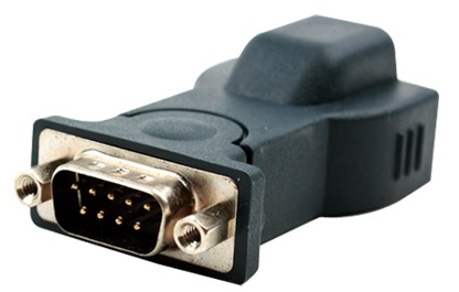
  RS-232 트랜시버 사용을 위해 BF810이라고 하는 USB to Serial 컨버터를 개조하여 사용 했다. [Fig. 2] 처럼 생긴놈을 분해하면 PL2303 USB 칩과 ADM213 RS-232 트랜시버 칩이 있는데 필요 없는 PL2303은 떼어 낸다. RCD-Programmer는 RS-232 신호중 TXD, DTR, RTS, CTS 신호선을 사용하므로 해당 신호선들을 찾아 CY7C68013의 PB[5:2] 포트와 연결한다. 펌웨어 개발은 일전에 공개한 debugbox 프로젝트에 포함 시켜 만들었다. AVRISP와 다르게 PIC 프로그래밍 프로토콜은 칩 모델마다 조금씩 다르게 구성 되어 있어 일반화된 프로그래밍 알고리즘 구현이 힘들다. 우선 'PIC12F629/675/PIC16F630/676 Memory Programming (DS41191D)' 메뉴얼의 프로그래밍 알고리즘을 구현하여 PIC16F676 디바이스로 테스트 해보았으며 [Fig. 8]와 같이 읽고 쓰기가 가능하였다.
  I used ADM213 RS-232 transceiver from BF810 USB to Serial converter. If you disassemble the BF810, you can see PL2303 and ADM213 chip on board. Remove PL2303 and connect to PB[5:2] port of CY7C68013A. In contrast to AVRISP, PIC programming algorithms are different from device to device. My initial implementation is for 'PIC12F629/675/PIC16F630/676 Memory Programming Manual (DS41191D)' and I could successfully read and write PIC16F676 device. Initial test code was developed with my debugbox project.

[Fig. 7] Integration

[Fig. 8] PIC16F676 R/W Test Result

[] Downloads
  - Pre-built firmware: Download
  - Source code: Download
  - just copy to debugbox project source directory and use it

debugbox

  debugbox는 개인 취미로 시작한 프로젝트로써 JTAG, SWD, AVR-ISP등 임베디드 시스템 개발시 필요한 USB 기반의 디버그 어댑터들의 모음이다. CY7C68013A USB 클라이언트 칩셋을 기반으로하는 단일 하드웨어에 아래 기능들을 모아 구현 하였다. 인터넷 어디선가 구할 수 있는 자료들을 기반으로 하였으며 소스가 있으면 해당 소스를 참고하여 포팅하고, 그렇지 못하면 관련 문서와 각종 포럼의 자료를 기반으로 그 기능을 모사 (emulation)하여 구현 하였다. 누군지도 모르는 웹 어디선가 자신의 삽질들을 공유 해준 덕분에 만들어 질 수 있었다. 내 삽질 또한 어느 누군가의 도움이 되길 바라며, 그간 진행해온 결과물을 소스 코드와 함께 공유한다. 좀더 나은 새로운 무언가가 만들어져 다시 또 내가 다른 형태의 도움을 받을 수 있는 선순환을 기대한다. (서두가 좀 거창한가?...)
  본 프로젝트에서는 사용자용 어플리케이션 소프트웨어를 새로 만들지 않는다. OpenOCD, avrdude등 기존에 잘 만들어져 사용되는 응용프로그램을 가능한 그대로 사용한다.

  소스코드와 미리 빌드된 펌웨어 다운로드 링크는 이 글 맨 아래쪽을 참고하면 된다.
  일반적인 JTAG 에뮬레이터의 TDI는 출력이고, TDO는 입력인데 타겟보드의 TDI는 이름 그대로 입력, TDO는 출력이다. JTAG 연합에서 왜 이렇게 만들었는지 모르겠으나 혼돈 스럽다. debugbox 프로젝트에서는 일반적인 JTAG 에듈레이터와 다르게 TDI는 모두 입력, TDO는 모두 출력으로 통일 시켰다.
  debugbox is my private project that is integration of useful USB based debug adapters such as JTAG, SWD, AVR-ISP and etcs with CY7C68013A USB client chip. My contribution is porting/migration/emulation and integration of USB debug bridge's firmware for CY7C68013A. In case of open-source based USB adapters, firmware is ported/migrated to CY7C68013A, if not, debug bridge functionalities are emulated through googled formal/informal documents and forum texts from World-Wide-Web with my trial and error. I'm sharing my debugbox project source code for hope to help someone who need it. 
Refer to download link at the end of this article.
  In general, target TDI is input and TDO is output but in JTAG emulator hardware, this naming is reversed. I have no idea why the JTAG assosiation defined such a confused naming. In my debugbox project, JTAG-TDI is input and JTAG-TDO is output.

[] debugbox features
  - USB-Blaster 1 (USB to JTAG)
    * UI Application: OpenOCD-JTAG (http://openocd.org)
    * Firmware: usb_blaster.ihx
  - USB-Blaster 2 (USB to JTAG)
    * UI Application: OpenOCD-JTAG (http://openocd.org)
    * Firmware: usb_blaster2.ihx
  - Versaloon-Link (USB to SWD)
    * UI Application: OpenOCD-SWD (http://openocd.org)
    * Firmware: vslswd.ihx
  - STK500 (USB AVRISP)
    * UI Application: avrdude (http://www.nongnu.org/avrdude)
    * Firmware: stk500.ihx
  - CP2112 (USB to SMBus/IIC)
    * UI Application: BE2Works (http://be2works.com)
    * Firmware: cp2112.ihx
  - JTAGIDER (JTAG pin identifier)
    * Firmware: jtagider.ihx


[Fig. 1] CY7C68013A Kit

[] Hardware
  앞서 이야기 한 것과 같이 USB 연동용 하드웨어는 CY7C68013A를 사용한다. [Fig. 1]와 같이 시중에 판매되는 CY7C68013A용 킷을 사다 사용해도 되고 나 처럼 CY7C68013A칩셋을 기반으로 하는 제품을 개조하여 사용 해도 된다. [Fig. 2]이 개조에 사용한 제품이며, Nvidia의 3D 비전용 적외선 방출장치를 개조하여 사용 하였다. VID/PID 저장용 IIC EEPROM은 제거 한다. PB[5:0]과 SMBus/IIC 통신을 위해 SCL/SDA를 인출 한다. 추가로 GND, 3.3V, 5V를 외부로 빼내어 하드웨어를 구성하면 된다. 개발을 위한 디버그 메시지가 필요하다면 UART 선도 외부로 인출하여 사용 한다.
  As I mentioned above, CY7C68013A is mandatory but IIC EEPROM (for VID/PID) is not needed. You may choose cheap CY7C68013A kit on the market for this project [Fig. 1]. In my case, I modified the commercial product IR emitter of 3D Vision which is CY7C68013A based small form factor housing from Nvidia [Fig. 2]. [Fig. 3] to [Fig. 6] are showing my modification. P1 is for probe pins and P2 is for 5V power output.

[Fig. 2] Nvidia IR Emitter for 3D Vision

[Fig. 3] PCB Top Side

[Fig. 4] PCB Bottom Side

[Fig. 5] Modification

[Fig. 6] Modification

[Fig. 7] Pull out PB[5:0], IIC and UART

[] P1 header pinout
  -------------------------------
   SDA  SCL  GND  RX0  TX0  3.3V
   PB0  PB1  PB2  PB3  PB4  PB5
  -------------------------------

[] Probe pin usage
  -------------------------------------------------------
   [PORT]  [JTAG]  [SWD]  [AVRISP]  [CP2112]  [JTAGIDER]
    PB5     TMS    SWDIO   -         -         Probe5
    PB4     TCK    SWCLK   SCK       -         Probe4
    PB3     TDO    -       MOSI      -         Probe3
    PB2     TDI    -       MISO      -         Probe2
    PB1     TRS    -       -         -         Probe1
    PB0     SRS    SRS     SRS       -         -
    SCL     -      -       -         SCL       -
    SDA     -      -       -         SDA       -
  -------------------------------------------------------

[] USB to SWD (Versaloon-Link)
  fxload를 이용해 'vslswd.ihx' 펌웨어를 CY7C68013A에 다운로드 하여 사용하면된다. 실제 Versaloon-Link 하드웨어는 출력 endpoint 주소로 0x03을 사용하여 구현되어 있다. 그러나 CY7C68013A 디바이스로 0x03 EP-OUT 구성이 불가능하여 'vslswd.ihx'펌웨어는 출력 endpoint로 0x04 주소를 사용해 구현 하였다. 때문에 OpenOCD의 소스 수정후 빌드하여 사용 해야 한다.
  CY7C68013A에 적재 가능한 코드 크기가 16KB로 제한되어 있어 모든 기능은 구현되지 않았으며 SWD 통신을 수행하는데 필요한 최소한의 기능만 구현되어 있다.
  Use 'vslswd.ihx' firmware for this function with fxload utility. The real Versaloon-Link's output endpoint address is 0x03, but 0x03 address is not applicable in CY7C68013A. Since I implemented output endpoint address as 0x04 instead 0x03 in 'vslswd.ihx', you should rebuild OpenOCD with modified address.
  Only SWD functions are implemented because of 16KB code memory limitation of CY7C68013A.

Edit OpenOCD source from
  ---------------------------------------------------------
   openocd/src/jtag/drivers/versaloon/versaloon_internal.h
   #define VERSALOON_OUTP 0x03
  ---------------------------------------------------------
to
  ---------------------------------------------------------
   openocd/src/jtag/drivers/versaloon/versaloon_internal.h
   #define VERSALOON_OUTP 0x04
  ---------------------------------------------------------


[Fig. 8] STM32F031 (from Syma 8X Drone) SWD Debugging

[] USB to JTAG (USB-Blaster 1/2)
  'usb_blaster.ihx' 혹은 'usb_blaster2.ihx' 펌웨어를 사용하여 OpenOCD와 연동하면 된다.
  Use 'usb_blaster.ihx' or 'usb_blaster2.ihx' with OpenOCD.


[Fig. 9] S5P6443 (from Car Navigation) JTAG Debugging

[] AVR-ISP (STK500)
  'stk500.ihx' 펌웨어와 avrdude를 사용하면 된다.
  Use 'stk500.ihx' firmware and avrdude.

[] USB to SMBus/IIC (CP2112)
  Silicon Labs의 CP2112라고 하는 'USB to SMBus/IIC' 컨버터를 모사한 기능으로 BE2Works 랩톱 배터리 모니터링 응용프로그램과 연동을 위해 만들었다. 'cp2112.ihx' 펌웨어를 사용하면 된다.
  This function is emulation of CP2112 USB to SMBus/IIC adapter from the Silicon Labs. You can communicate laptop battery with 'cp2112.ihx' firmware and BE2Works. I tested with demo version of BE2Works but the licensed version supports laptop battery reset, so you can replace battery cell by resetting error status and cycle count.

[Fig. 10] BE2Works

[Fig. 10] Laptop Battery Monitoring

[] JTAG Pin Identifier
  이 기능은 임베디드 보드의 JTAG 핀 배열을 모를때 TMS, TCK, TDO, TDI, TRS 핀의 위치를 자동으로 찾아주는 기능이다. 'jtagider.ihx'를 사용하면 되고 PC에서는 VCP (Virtual COM Port)로 인식된다. 해당 포트를 Teraterm과 같은 터미널로 연결하여 명령어를 입력하는 방식이다. [Fig. 11]은 [Fig. 9]의 메인보드상 S5P6443의 JTAG 핀 배열을 찾아낸 결과를 보여주고 있다. 보통 JTAG-TAP들은 Daisy-Chain 방식으로 연결 되어 있어 연결 방식을 감안하여 숫자를 입력 한다. S5P6443의 경우 ETM과 ARM 2개의 JTAG-TAP이 연동 되어 있으며 각 IR의 길이는 4-bit와 5-bit이다. 명령 입력은 '[pre-dcnt] [pre-irlen] [inst-len] [post-dcnt] [post-irlen]' 순서로 숫자만 입력한다. '0 0 4 1 5' 명령으로 ETM-TAP의 ID인 '0x2B900F0F'가 확인 되었으며 이때 핀 배열은 'RIOCM (Probe1~5:TRS/TDI/TDO/TCK/TMS)'로 확인 된다. '1 4 5 0 0' 명령으로 ARM11-TAP의 ID인 '0x07B76F0F'가 확인이 되고 핀 배열은 동일한 'RIOCM (
Probe1~5:TRS/TDI/TDO/TCK/TMS)'로 확인 되었다.
  You can use this function to identify JTAG pin order for unknown target board. Download firmware 'jtagider.ihx' and you may found a new VCP (Virtual COM Port) on your PC after download it to CY7C68013. Connect to that COM port with terminal emulator such as Teraterm and you can see prompt 'JID'. [Fig. 11] is my example result of [Fig. 9] S5P6443 based car navigation board. That board has JTAG port but the pin order is unknown. In the S5P6443 reference manual, there are daisy-chained 2 JTAG-TAPs, ETM and ARM11. Command order is '[pre-dcnt] [pre-irlen] [inst-len] [post-dcnt] [post-irlen]'. I could identify JTAG pin order 'RIOCM (Probe1~5:TRS/TDI/TDO/TCK/TMS)' by command '0 0 4 1 5' with detected ETM-TAP ID '0x2B900F0F'. Command '1 4 5 0 0' shows same JTAG pin order 'RIOCM (Probe1~5:TRS/TDI/TDO/TCK/TMS)' with detected ARM11-TAP ID '0x07B76F0F'.


  ----------------------------------------------
                 ETM-TAP       ARM11-TAP
                +--------+    +--------+
   JTAG_TDO ----+TDI  TDO+----+TDI  TDO+---+
                +--------+    +--------+   |
                 IR-4bit       IR-5bit     |
                                           |
   JTAG_TDI -------------------------------+

            [S5P6443 JTAG-TAP Chain]
  ----------------------------------------------

  * pre-dcnt  : Total device count of front side daisy-chain
  * pre-irlen : Total IR bit-length of front side daisy-chain
  * inst-len  : IR length to check ID
  * post-dcnt : Total device count of end side daisy-chain
  * post-irlen: Total IR bit-length of end side daisy-chain

[Fig. 11] S5P6443 Car Navigation Board JTAG Pin Identification

  CY7C68013의 아주 유용한 기능중 하나가 로직어날라저로 사용이 가능한데 sigrok (https://sigrok.org)을 사용하면 무려 16채널 24MHz 로직 어날라이저로도 사용 가능하다.
  Another very useful function is logic analyzer, you can check the sigrok (https://sigrok.org) to use the CY7C68013 as 16-Ch. 24MHz logic analyzer.

[] Downloads
  - Pre-built firmware: Download
  - Source code
: Download
  - Compiler used: sdcc-3.9.0

  소스는 개인적인 목적이라면 자유롭게 사용/수정/재배포 가능하며, 상업적 이용은 금지합니다.
  You can freely use/modify/republish my source code for private purpose, but DO NOT USE for commercial product. 

맞는 말


노무현없는 노무현시대...


노무현: "노무현의 시대가 오겠어요?"
유시민: "오지요. 100% 오죠 그거는. 반드시 올 수밖에 없죠."
노무현: "아, 근데 그런 시대가 오면 나는 없을거 같아요."

2018/09/26 ~ 10/05 몰디브여행


결혼하고 푸켓 신혼여행때
'우리 결혼 10주년에는 몰디브 한번 가보자' 했던,
와이프와의 10여년전 약속을 지켰다.
그 사이 생겨난 딸아이 둘과 함께...


한국에 도착하자마자
니글니글한 속을 달래주기위해
순식간에 흡입한
짬뽕 한 그릇에  막걸리 한 병
(인천공항 제2터미널 푸드코트)


늬들이 이 물속에서 오줌싸는 기분을 알아?


또 가고 싶다 몰디브...

뭘까?


블로그 설정 화면에서 내 블로그를 방문하는 사람들의
접속 국가별 페이지를 제공하는데,
가끔씩 저렇게 러시아 접속자가 많을 때가 있다.
생각해 보니 자주인거 같기도...

뭘까?

러시아어로 써놓은 게시물도 없고,
영어로 써놓은 게시물이 많지도 않은데...

러시아 거쳐서 오는 사람들인가?
러시아에 우회 서버가 많은가?
정원이 인가?
갑자기 무서워짐
난 콩사탕이 싫어요!!~~

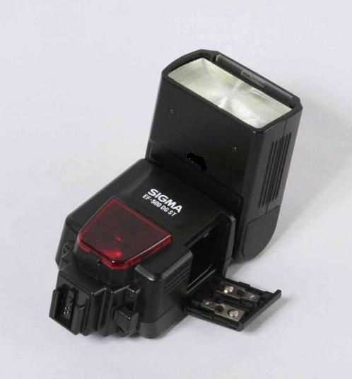
Sigma EF-500 DG SUPER MA(Minolta) Modification for the Pentax Hot Shoe Mount

이번 삽질도 아트와 관련된 거다.
내가 원래 아트에 관심이 좀...

재활용 쓰레기통에서 망가진 외장 플래시를 구했다.
모델명은 'Sigma EF-500 DG SUPER MA'로 보인다.
확인해 보니 플래시 램프가 타버렸다.
가지고 있는건 펜탁스 카메라인데, 이건 Minolta 마운트용이다.
[Fig. 1] 처럼 생겼다.

I've finished the conversion of the 'Sigma EF-500 DG SUPER MA' Minolta hot shoe mount into the Pentax hot shoe mount. And I'll describe what I've done about it.
My Sigma EF-500 DG SUPER MA's flash lamp was burned out so doing the lamp replacement is initial process and then, I have to modify mechanical-mounting followed by electrical-mounting.
I did not took pictures during the flash lamp replacement.


[Fig. 1 Sigma EF-500 DG Minolta Mount]

펜탁스에 붙여서 사용하려니 3가지 작업을 해야한다.

1. 타버린 램프를 교체
2. 기계적 마운트롤 교체
3. 전기적 마운트도 교체

음.. 일이 많다.
가지고 있던 싸구려 외장 플래시에서 램프를 빼내어 교체작업을 한다.
플래시 분해는 아래 사이트를 참고 했다.

You can refer to below link to disassemble the strobe.

Repairing an erratic Sigma EF500 DG ST
(Thank you weijen)


[Fig. 2 Extracted Burned Flash Lamp]


[Fig. 3 Hot Shoe Mount Replacement]

교체후 타버린 플래시 램프 사진만 찍었다
램프 교체하고 테스트를 해보니 동작은 잘 된다.
기계적 마운트역시 가지고 있던 외장 플래시에서 마운트 부분을 떼어내 붙여 준다.
자, 이제 전기적 마운팅을 해줘야 하는데 자료를 뒤져 보니 이거 만만치가 않다.
그냥 strobe signal을 접지 시키면 될 줄 알았는데 그렇지가 않다.
특히나 Minolta 방식이 까다로운가 보다.
전기적 마운팅을 위해 아래 3개 사이트를 참고 했다.

I've checked it works well after repairing the flash lamp, and have modified the mechanical mount with parts from my cheap external strobe for the Pentax.
Next step is just electrical-mounting but I've been aware of danger of this job. There are no easy way to trigger this strobe manually just like shorting the fire signal to the ground.
I've found out very useful 3 links bellow for this.

adrian        : Hacking the Sigma EF-500 DG Super strobe Part 1/2
Kimmo Kulovesi: Sigma EF-500 DG Super PC-sync port modification
Impulsite     : Sigma EF-500 DG ST, есть схема
(Thank you adrian, Kimmo Kulovesi and Impulsite)

adrian 링크는 수동으로 플래시를 동작 시키기 위해 겪은 시행착오를 공유해 놓은 내용이고 Kimmo Kulovesi 링크는 adrian의 시행 착오에 15nF 커패시터를 추가하여 개선했다는 내용이다. Impulsite 링크는 플래시 회로도를 공유해 주었다.
3명의 자료 공유 덕분에 내 작업이 비교적 순조롭게 진행 될 수 있었다.
얼굴도 모르는 세계의 3분에게 다시한번 감사드린다. 소중한 시간을 아낄 수 있었다.

I think the adrian is a pioneer of the Sigma EF-500 DG modification. He suggested really good idea for manual trigger through the optical-slave mode of the strobe and this method works well. All images are broken when I visit the adrian's site, but you can search images by image-googling with 'Hacking the Sigma EF-500 DG Super strobe' key words.
Kimmo Kulovesi improved the unstable behavior by attaching 15nF capacitor for bypassing noise, also very nice recommendation.
Impulsite's web is very useful with strobe's schematics.
I could make a conversion into the Pentax mount successfully by these informaion only in 2 days. I hope to say thank you adrian, Kimmo Kulovesi and Impulsite again, you saved my time.
Additionally, I performed several invetigation and experiments to make it clear. When I shorted the photo-diode's anode and cathod, large current was observed by probing the voltage drop with my strobe, so I added current limiting register in my final result, R1 in [Fig. 7].
General Si. photo-diodes let current under 100uA, typically 50~60uA, when detected the light.
The main CPU should observe the delta-voltage, approximatly under a hundred micro-volts to detect the light if there is no signal amplification.
I found that the photo-diode's singal (anode) is routed to the main CPU(?) directly, it's means that the main CPU(?) may detect under 100uV of delta-volts to sync with light signal when it's in optical-slave mode.
The strobe's unstable behavior (without Kimmo Kulovesi's 15nF capacitor) could be explained by this measurement mechanism. If you extended the photo-diodes's signal wire (anode), even small disturbances could influence the delta-micro-volts detection loop so the Kimmo Kulovesi's 15nF capacitor is very important.
To protect DSLR camera I attached the opto-coupler PC817.
You should short pin 5 and 6 to work properly in optical-slave mode. refer to [Fig. 8].
My Pentax camera and the modified Sigma EF-500 DG SUPER MA works perfectly togather in "C0 SL" mode.

요약하자면 다음과 같다.

1. Sigma EF-500 DG SUPER는 단순 단락으로 플래시 동작이 안된다.
2. optical-slave모드에서 내부 photo-diode 신호를 변형해 동작이 가능하다.
3. photo-diode 신호 변형을 위해 wire를 인출 하면 동작이 이상해 진다.
4. 인출된 wire에 커패시터를 부착하면 사용가능한 수준이 된다.

adrian이 말한대로 photo-diode에서 선을 빼내면 수동으로 동작이 가능하지만, 가끔 플래시가 먹통이 된다. 이를 위해 Kimmo Kulovesi는 신호선에 15nF 커패시터를 달아 해결하였다.
Impulsite의 회로도를 참고해 나름 테스트를 해본 결과 photo-diode의 신호를 메인 CPU(?)에서 입력 받는 구조인데, photo-piode의 전류 신호가 수십 uA대로 작다 보니 측정되는 전압의 변화 역시 수십uV 수준이다.
외부에 선을 달아 주게 되면 안테나 역할을 하게 되면서 외부 노이즈가 유입되어 플래시 커패시터의 방전과 충전이 반복되면서 기기가 먹통이 된다.
처음에 adrian이 소개한 대로 photo-diode의 선을 인출 하여 쇼트시켜보니 동작은 하는데 전류가 많이 흐르는듯 하다. 하여, 아래와 같이 카메라도 보호할 겸해서 opto-coupler를 추가로 장착하여 카메라와 연동하는데 성공 했다. [Fig. 7]에서 추가한 R1은 과전류 보호용이고 R2는 opto-coupler의 발광 다이오드 구동용이다.
optical-slave 모드로 동작 시키기 위해서는 [Fig. 8]과 같이 커넥터 5번과 6번을 쇼트 시켜야 한다.
플래시의 발광량 가변이 되니 신세계다.


[Fig. 4 Power board, Pic. from Impulsite]


[Fig. 5 Power board Schematics, Pic. from Impulsite]


[Fig. 6 Photo-Diode Polarity, Anode(A) and Cathod(C)]


[Fig. 7 Modification Schematics]


[Fig. 8 Connector Modification]

Hot shoe connector pin out
  - 1  : F2 (READY)
  - 2  : F1 (SYNC/FIRE)
  - 3  : GND
  - 4  : F3 (TTL OK)
  - 5/6: Shoe Mount Detection (contacted together when demounted)
  - 7/8: LED

[Fig. 9 Wiring]


[Fig. 10 Final Result]

사진은 안찍고 이런거나 만들고 있음.